|
Jungo WinDriver
Official Documentation
|
|
Jungo WinDriver
Official Documentation
|
In addition to the standard WinDriver APIs and the DriverWizard code generation capabilities described in this manual, which support development of drivers for any PCI/ISA device, WinDriver features enhanced support for specific PCI chipsets. This enhanced support includes custom APIs, customized code generation (for some of the chipsets), and sample diagnostics code, which are all designed specifically for these chipsets.
The table below outlines the PCI chipsets and FPGA PCIe IPs that WinDriver provides enhanced support for, and indicates which of them offer customized code generation:
| Vendor | Sample | Customized Code Generation Support |
|---|---|---|
| PLX | 6466, 9030, 9050, 9052, 9054, 9056, 9080, 9656 | No |
| Altera | mSGDMA | Yes |
| Altera | mSGDMA Platform | Yes |
| Altera | Avalon-MM | Yes |
| Altera | Avalon-MM Scaler | Yes |
| Altera | MCDMA | Yes |
| Xilinx | BMD | Yes |
| Xilinx | XDMA | Yes |
| Xilinx | QDMA | Yes |
| Lattice | CertusProNX SGDMA PCIe IP | Yes |
| Lattice | Avant DMA Bridge Core PCIe IP | Yes |
When developing a driver for a device based on one of the enhanced-support chipsets described above, you can use WinDriver's chipset-set specific support in the following manner: if your device is based on one of the designs listed above you can generate customized code for the device by selecting this option in the DriverWizard code generation options dialogue (see 6.2. DriverWizard Walkthrough). Alternatively, or if you are using another enhanced-support device, follow the steps below to use one the enhanced-support WinDriver samples as the starting point for your development:
WinDriver/samples/language/chip_vendor/chip_name directory.Most of the sample diagnostics programs are named xxx_diag and their source code is normally found under an xxx_diag subdirectory. The program's executable is found under a subdirectory for your target operating system (e.g., WIN32 for Windows.)
WinDriver/samples/language/chip_vendor/lib directory.Starting from version 12.3, WinDriver supplies a user-mode sample code of a diagnostic utility that demonstrates several features of Xilinx PCI Express cards programmed with a Xilinx DMA IP.
The sample source code and the pre-compiled sample can be found in the
WinDriver/samples/c/xilinx/xdma directory.
Before running the diagnostic utility, make sure that DriverWizard is closed, to avoid a “resource overlap” error.
⚠ Attention
If you have a proper XDMA supporting device attached, the diagnostic
utility might open it automatically on startup, as shown here. Otherwise, you can choose option 2 and to try to open a device yourself.
The xdma_diag utility

The XDMA sample code is built on the XDMA default example design. For more details about this design refer to the DMA/Bridge Subsystem for PCI Express Product Guide - AXI4 Memory Mapped Default Example Design
The XDMA design is compatible with the following device families:
| Compatible Device Family |
|---|
| UltraScale |
| UltraScale+ |
| 7 Series Gen2 devices |
| Spartan UltraScale+ |
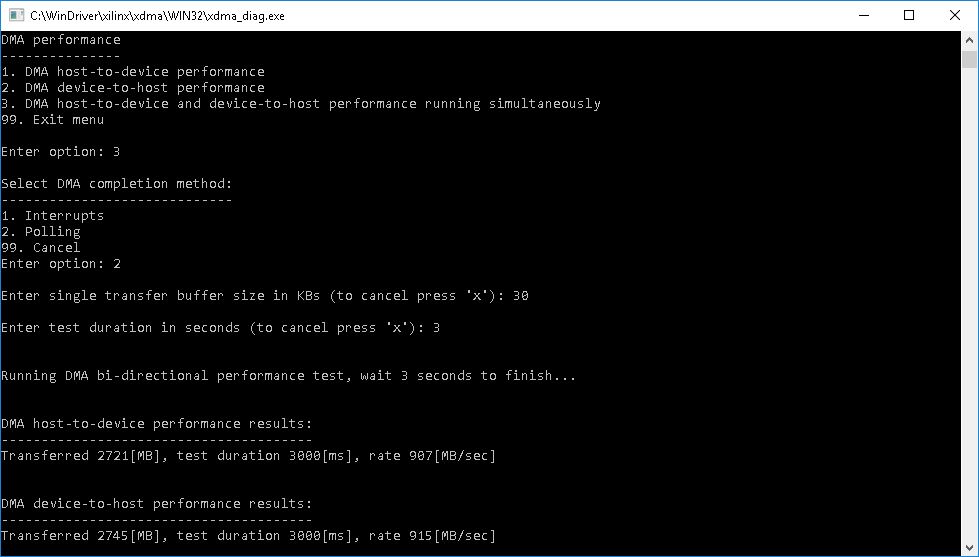
After choosing option 6 from the XDMA main menu, the user can either Perform a DMA transfer or Measure DMA Performance.
The DMA transfer option allows the user to actually read or write data from device.
The writing option prompts the user to type a hexadecimal 32 bit packet of data, and this packet is repeatedly written to the device’s memory, according to the user entered Number of packets to transfer. The reading option prints out the contents of a certain memory area, according to the user entered FPGA offset.
A simple test can be:
XDMA Transfer example
The DMA performance option allows the user to test the speed of the device. The user is prompted to choose a transfer direction (to device, from device, or simultaneous bi-directional transfers). Then the user is prompted to enter a buffer size for the each transfer that will be made during the test, and the test’s duration. Afterwards the test takes place and in the end of the test the results will be printed out.
XDMA Performance test example
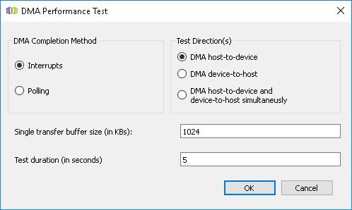
Starting from WinDriver version 12.5, WinDriver also supplies a GUI utility, based upon the same xdma_diag source code, showcasing the above mentioned DMA Transfer and DMA Performance tests. The xdma_gui utility can be found in the WinDriver/samples/c/xilinx/xdma/gui directory. Similar to the console xdma_diag program, the xdma_gui utility will try to open an XDMA device automatically, and if it will fail then it will be required to first select and open an XDMA-supported device before being able to perform the tests.
The xdma_gui Utility

DMA Transfer test in xdma_gui
DMA Performance in the xdma_gui Utility
Starting from WinDriver version 12.5, DriverWizard allows generating a user-mode diagnostics program source code that is similar to the supplied xdma_diag program, by choosing Xilinx XDMA design from the Add device specific customization (optional) menu.
See 6.2.9.1. Samples Or Code Generation for more information.
Starting from version 14.4 WinDriver supplies a cross-platform user-mode sample code of a diagnostic utility that demonstrates several features of Xilinx PCI Express cards with QDMA IP (Multi Queue DMA) support.
The sample source code and the pre-compiled sample can be found in the
WinDriver/samples/c/xilinx/qdma directory.
Before running the diagnostic utility, make sure that DriverWizard is closed, to avoid a “resource overlap” error.
⚠ Attention
If you have a QDMA supporting device attached, the diagnostic utility will open it automatically on startup. Or you can choose “Find and open a QDMA device” option to try to open a device yourself.
The QDMA sample code is built on the QDMA AXI Memory Mapped Example Design. For more details about this design refer to the QDMA Subsystem for PCI Express Product Guide - AXI Memory Mapped Example Design
The QDMA design is compatible with the following device families:
| Compatible Device Family |
|---|
| UltraScale+ |
| Spartan UltraScale+ |
After choosing “Direct Memory Access (DMA) transaction” option, the user can either Perform a DMA transaction. The DMA transaction option allows the user to actually read or write data from device.
In order to do this you will need to:
If you selected Blocking method you can see the transaction details (including transaction rate) when it is finished, otherwise (Non-blocking method), you can see it in the Requests sub-menu.
Several QDMA devices can be opened simultaneously. To switch between physical functions select “Change physical function” in the menu.
The following actions may be done on the Requests menu:
In order to get queues status (Available/Programmed/Started), select “Get queue status”.
Starting from WinDriver version 14.4, DriverWizard allows generating a user-mode diagnostics program source code that is similar to the supplied qdma_diag program, by choosing Xilinx QDMA design from the Add device specific customization (optional) menu.
See 6.2.9.1. Samples Or Code Generation for more information.
Starting from version 16.6 WinDriver supplies a Linux user-mode sample code demonstrates several features of Xilinx AXI DMA IP when using on SoC.
The sample source code and the pre-compiled sample can be found in the
WinDriver/samples/c/xilinx/axidma directory.
Before running the diagnostic utility, make sure that DriverWizard is closed, to avoid a “resource overlap” error.
| Compatible Device Family |
|---|
| Versal ACAP |
| UltraScale+ |
| UltraScale+ |
| Zynq-7000 SoC |
| Xilinx 7 Series FPGAs |
See Chapter 18: SoCs and Platform Devices for more information about platform devices.
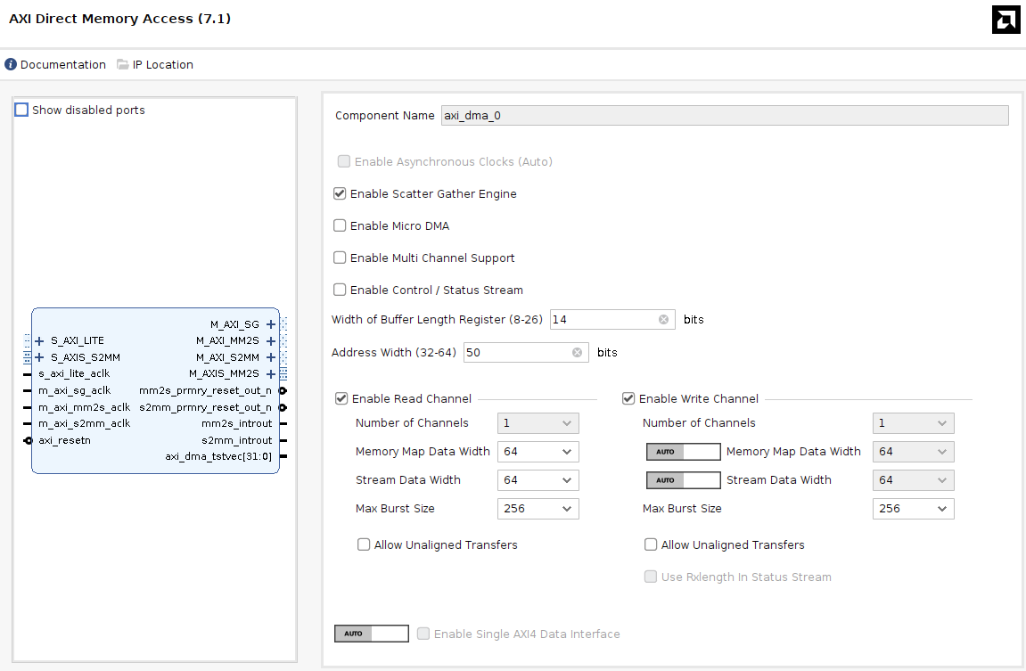
The AXI DMA sample is based on an FPGA design where the AXI DMA core interfaces between a Zynq processor and an AXI BRAM Controller. The following image from Vivado (Hardware Design Software by AMD) illustrates the core configuration parameters:
To facilitate Memory-to-Memory (M2M) DMA operations, the streaming interfaces are configured in a loopback arrangement. This setup allows data to be moved between memory locations by routing the output stream directly back into the input stream. The following image from Vivado (Hardware Design Software by AMD) displays the AXI DMA streaming loopback configuration:
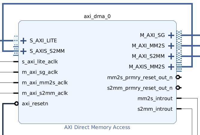
The AXI DMA IP utilizes three distinct AXI4 interfaces for data and descriptor management:
M_AXI_SG - A dedicated interface used by the DMA engine to fetch and update Scatter-Gather descriptors from the processor's memory.M_AXI_MM2S - A master interface that reads data from memory and transmits it to the M_AXIS_MM2S streaming interface.M_AXI_S2MM - A master interface that receives data from the S_AXIS_S2MM streaming interface and writes it to memoryIn this sample design, the connectivity is structured as follows:
M_AXI_SG interface is connected to a slave AXI4 interface on the Zynq processing system.M_AXI_MM2S and M_AXI_S2MM interfaces share the same slave interface as the M_AXI_SG. Additionally, they are connected to an AXI BRAM controller, enabling high-speed read/write access to on-chip memory.The AXI DMA IP generates two separate level-triggered interrupts: mm2s_introut (transmit) and s2mm_introut (receive).
In this implementation, these two signals are consolidated into a single interrupt line using a logical OR gate. This combined output is then connected to the Zynq interrupt input. This configuration is required because current WinDriver samples are designed to support a single interrupt per IP core.
For WinDriver to correctly identify and manage the AXI DMA IP, the following device node must be incorporated into the system's Device Tree. Use the template below, replacing the bracketed placeholders with the specific values from your hardware design:
The following example illustrates the device node used for the Kria KV260 implementation:
DriverWizard allows generating a user-mode diagnostics program source code that is similar to the supplied axidma_diag program, by choosing Xilinx AXI-DMA design from the Add device specific customization (optional) menu after choosing your platform device.
See 6.2.9.1. Samples Or Code Generation for more information.
Starting from version 11.1 WinDriver supplies a cross-platform user-mode sample code of a diagnostic utility that demonstrates several features of Altera Modular Scatter Gather DMA IP.
This sample supports the following hardware design configurations:
The mSGDMA sample is based on an example design that can be adapted to any Altera device family. The sample is intended for use with one of the following PCIe IP cores and their compatible device families but can be used also with other IPs when the mSGDMA IP is an additional DMA engine:
| PCIe IP Core | Compatible Device Family |
|---|---|
| IP Compiler for PCIe | Arria II GX/GZ, Cyclone IV GX, Stratix IV E/GX/GT |
| V-Series Avalon-MM Hard IP for PCIe | Arria V, Stratix V, Cyclone V |
| 10-Series Avalon-MM for PCIe (DMA disabled) | Arria 10, Cyclone 10 |
| H-Tile/L-Tile Avalon MM for PCIe (DMA disabled) | Stratix 10 |
The design includes two main IP cores:
WinDriver recommends using the mSGDMA example design in cases where:
To create this design using Quartus and Platform Designer:
The sample locks a single contiguous DMA data buffer and a single contiguous DMA descriptors buffer.
The descriptors buffer contains two descriptors:
To initiate a transfer, each descriptor is submitted to the dispatcher core. When the MSGDMA_DESC_CONTROL_GO_BIT is set, the dispatcher processes the descriptor.
For 64-bit addressing, the the extended feature descriptor format is used.
The sample locks a single scatter-gather DMA data buffer and a single contiguous descriptor buffer.
Each descriptor includes a next pointer, creating a linked list of descriptors. The prefetcher core is configured with the address of the first descriptor. Once the MSGDMA_PREFETCHER_CONTROL_RUN_BIT is set, the prefetcher begins fetching descriptors until it reaches one that is not marked as owned by hardware (MSGDMA_DESC_CONTROL_OWNED_BY_HARDWARE_BIT).
To check for completion, software polls the prefetcher MSGDMA_PREFETCHER_CONTROL_RUN_BIT.
DriverWizard allows generating a user-mode diagnostics program source code that is similar to the supplied msgdma_diag program, by choosing Altera mSGDMA design from the Add device specific customization (optional) menu.
To generate code for your specific design, select the desired configuration from the Select Additional Options menu:
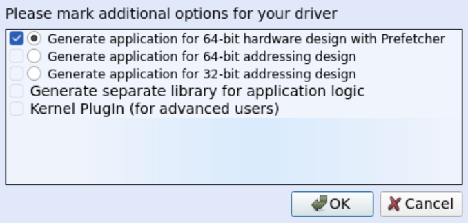
See 6.2.9.1. Samples Or Code Generation for more information.
Starting from version 16.6 WinDriver supplies a Linux user-mode sample code of a diagnostic utility that demonstrates several features of Altera Modular Scatter Gather DMA IP when using on SoC.
This sample supports the following hardware design configurations:
See 9.6. The mSGDMA sample code for more information about the msgdma sample.
See Chapter 18: SoCs and Platform Devices for more information about the drivers for SoC.
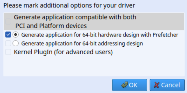
DriverWizard allows generating a user-mode diagnostics program source code that is similar to the supplied msgdma_platform_diag program, by choosing Altera mSGDMA design from the Add device specific customization (optional) menu after choosing your platform device.
To generate code for your specific design, select the desired configuration from the Select Additional Options menu:
See 6.2.9.1. Samples Or Code Generation for more information.
Starting from version 14.7, WinDriver supplies a user-mode sample code of a diagnostic utility that demonstrates several features of Intel Altera PCI Express cards programmed with a Avalon-MM IP.
The sample source code and the pre-compiled sample can be found in the
WinDriver/samples/c/altera/avalonmm directory.
The Avalon-MM sample code is built on a design which connects the Avalon-MM DMA for PCIe IP with an On-chip memory IP. The IPs are connected using both the DMA and one of the RXM interfaces.
The Avalon-MM Sample is compatible with the following IPs:
| PCIe IP Core | Compatible Device Family |
|---|---|
| Avalon-MM Interface for PCI Express | Arria 10, Cyclone 10 |
| H-Tile/L-Tile Avalon-MM Hard IP for PCI Express | Stratix 10 |
DriverWizard allows generating a user-mode diagnostics program source code that is similar to the supplied avalonmm_diag program, by choosing Altera Avalon Memory Mapped (Avalon-MM) design from the Add device specific customization (optional) menu.
See 6.2.9.1. Samples Or Code Generation for more information.
Starting from version 16.5 WinDriver supplies a cross-platform user-mode sample code of a diagnostic utility that extends the WinDriver's Avalon-MM sample code with features for transferring an image to a DDR memory on the PCIe device and uses Altera’s Scaler II IP to upscale or downscale the image dimensions.
The sample source code and the pre-compiled sample can be found in the WinDriver/samples/c/altera/avalonmm_scaler directory along with an archive file that contains a Quartus project of the Scaler Example Design and a pre-compiled bitstream which is ready to be programmed on a Cyclone 10 GX FPGA Development Kit. For more details about that development kit refer to the Cyclone® 10 GX FPGA Development Kit.
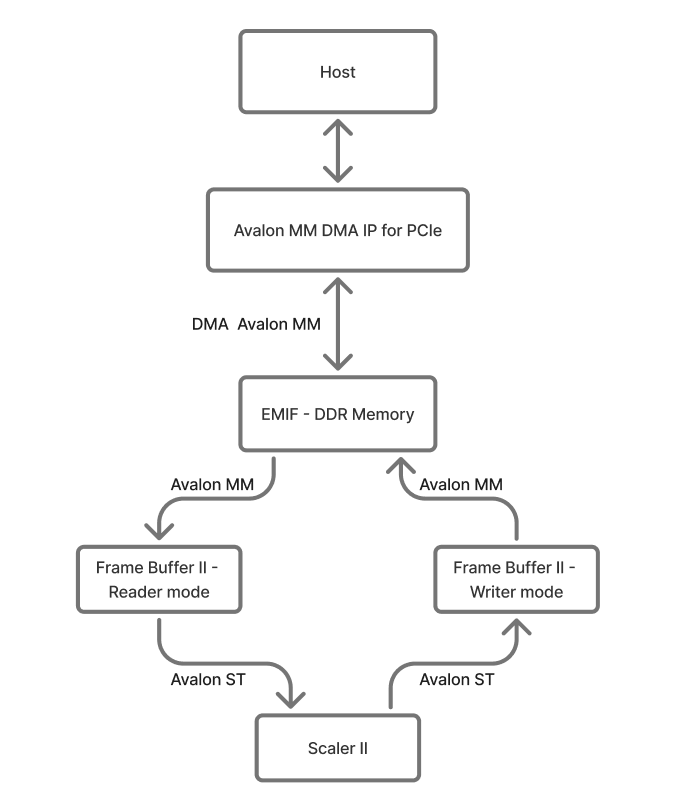
The Scaler Example Design integrates several Altera IPs, including the Avalon-MM DMA for PCIe, the External Memory Interface (EMIF), two instances of the Frame Buffer II (one in Reader mode and one in Writer mode), and the Scaler II IP.
When scaling an image with the Avalon-MM Scaler sample, the process begins by transferring the image to the DDR memory through the Avalon-MM DMA for PCIe IP. The Frame Buffer in Reader mode IP then retrieves the image from the DDR memory and streams it to the Scaler II IP. Based on the user’s selection in the application, the Scaler II IP upscales or downscales the image and streams the result to the Frame Buffer in Writer mode IP. This Frame Buffer writes the scaled image back into DDR memory. Finally, the application detects when the scaled image is ready in memory and retrieves it to the host using the Avalon-MM DMA for PCIe IP.
The Example Design is straightforward and can be adapted to any Altera FPGA device that supports the Avalon-MM DMA IP for PCIe. An archive containing the Quartus project is available in the sample’s directory within the WinDriver installation path (samples/c/altera/samples/c/altera/avalonmm_scaler). The project should be extracted and modified for the target FPGA device. Key areas to update include:
When the example design is modified or DDR memory of a different size is used, specific C macros may need to be updated:
vfb_lib.h.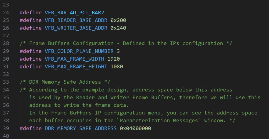
scaler_lib.h.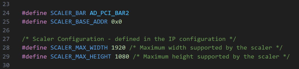
avalonmm_image_lib.h.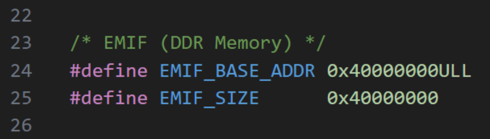
Program the FPGA using either the provided Scaler Example Design bitstream or a custom bitstream.
Navigate to the avalonmm_scaler directory in the samples directory of the WinDriver installation and run the sample avalonmm_scaler_diag.
The sample will launch and display the main menu. If the device does not open automatically, the programming may have failed, or (on Windows) a required INF file may be missing. To install an INF file, see 17.1. Windows INF Files
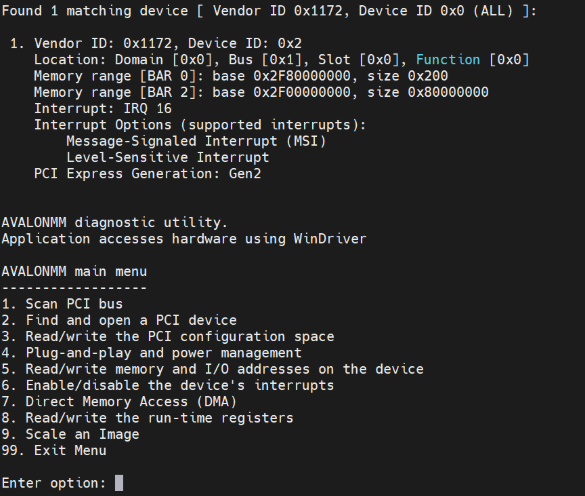
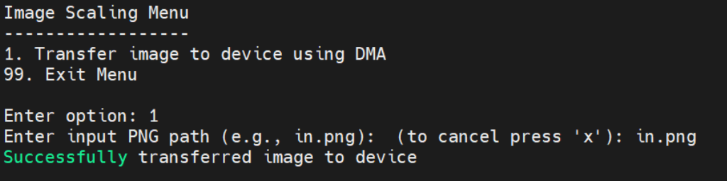
Option 9 in the main menu provides access to the image scaling menu.
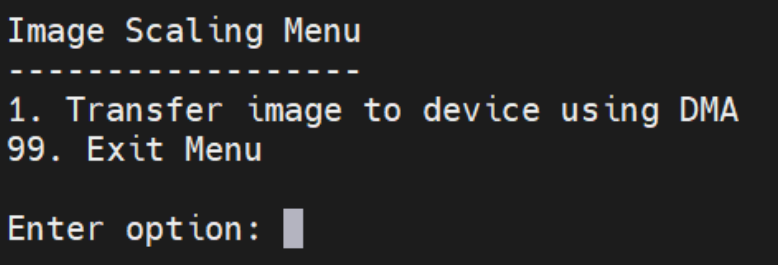
In the Image Scaling Menu, three options are presented in sequence. Initially, only option 1 is visible. Selecting this option prompts you to enter the path of an image, which will then be opened and transferred to the FPGA card.
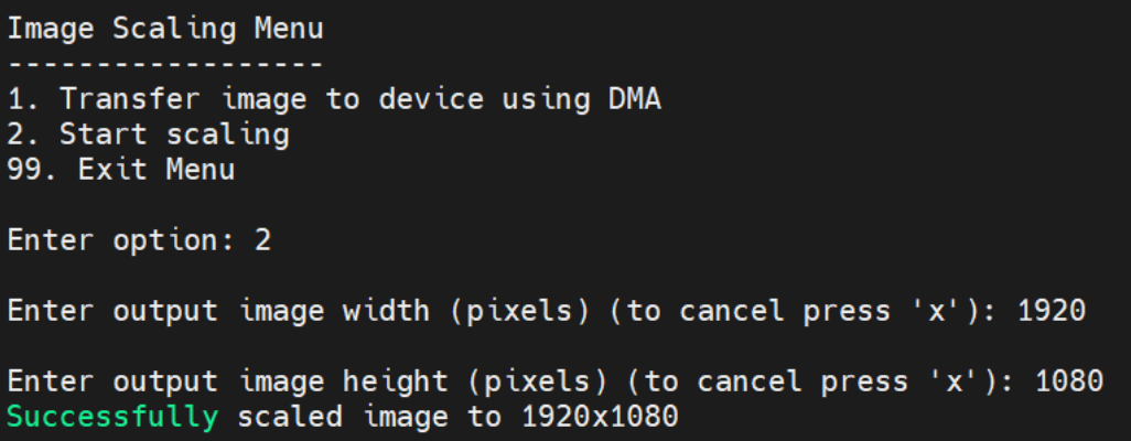
After successfully completing option 1, option 2 becomes available to scale the image. The application prompts for the target dimensions and then starts the scaling process. Note that the first run may take a few seconds.
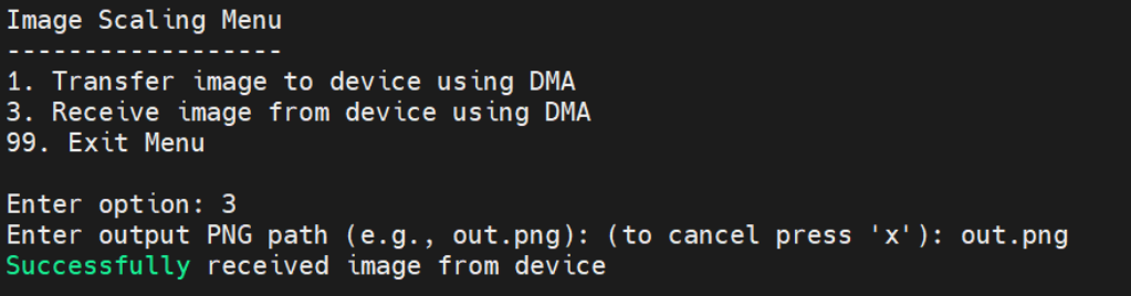
After the scaling process is complete, option 3 becomes available to retrieve the image from the device. The application prompts for an output path and saves the scaled image to the specified location on the host machine.
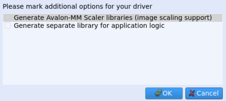
DriverWizard allows generating a user-mode diagnostics program source code that is similar to the supplied avalonmm_scaler_diag program, by choosing Altera Avalon Memory Mapped (Avalon-MM) design from the Add device specific customization (optional) menu and then selecting the Generate Avalon-MM Scaler libraries (image scaling support) option from the Select Additional Options menu:
See 6.2.9.1. Samples Or Code Generation for more information.
Starting from version 16.5 WinDriver supplies a cross-platform user-mode sample code of a diagnostic utility that demonstrates several features of Altera Multi Channel DMA IP.
This sample demonstrates the use of a single scatter-gather buffer for DMA data, along with a single contiguous buffer for the DMA descriptors that describe the memory transfers.
The descriptor buffer is organized as a circular list:
Note: The total number of descriptors must be a power of 2. Therefore, for a scatter-gather DMA data buffer with n contiguous segments, the software automatically allocates and locks the next power of 2 descriptors.
Each descriptor specifies:
The Altera Multi Channel DMA IP. supports several completion methods:
The MCDMA sample works with several Altera IP cores, including:
| DMA IP Core | Tile Variant | Compatible Device Families |
|---|---|---|
| Avalon MCDMA IP | H-Tile, P-Tile, F-Tile, R-Tile | Stratix 10, Agilex 7, Agilex 9 |
| AXI MCDMA IP | R-Tile | Agilex 7 I-Series |
| GTS AXI MCDMA | Agilex 5 |
DriverWizard allows generating a user-mode diagnostics program source code that is similar to the supplied mcdma_diag program, by choosing Altera MCDMA design from the Add device specific customization (optional) menu.
See 6.2.9.1. Samples Or Code Generation for more information.
Starting from version 16.4 WinDriver supplies a cross-platform user-mode sample code of a diagnostic utility that demonstrates several features of Lattice CertusProNX SGDMA PCIe IP support.
This sample locks a single scatter-gather buffer for DMA data and a single contiguous buffer for the descriptors describing the memory transfer that should be transformed. Each descriptor holds a source address, a destination address, the length of the current data block, the address of the next descriptor and control bits (to control EOP/Interrupt).
The Lattice CertusProNX SGDMA PCIe IP supports 2 MSI interrupt vectors, the interrupt vector used is set by writing to H2F/F2H_INT_VEC register.
A DMA transfer is initiated by setting bit CPNXDMA_START_DMA of H2F/F2H_SGDMA_CTRL register.
| Compatible Device Family |
|---|
| CertusProNX |
The diagnostic utility includes a 'Direct Memory Access (DMA)' menu which includes the sub-menus:
ℹ️ Note
All the above operations can be done using a Kernel Plugin (for higher performance) as well as without a kernel plugin.
DriverWizard allows generating a user-mode diagnostics program source code that is similar to the supplied cpnxdma_diag program, by choosing 'Lattice CPNXDMA design' from the Add device specific customization (optional) menu.
See 6.2.9.1. Samples Or Code Generation for more information.
Starting from version 16.4 WinDriver supplies a cross-platform user-mode sample code of a diagnostic utility that demonstrates several features of Lattice Avant DMA Bridge Core PCIe IP support.
This sample locks a single scatter-gather buffer for DMA data and four contiguous buffers for:
The S/G source address and S/G destination address queues describe the fragmentation of the source and destination memory transfer respectively.
The Lattice Avant DMA Bridge Core PCIe IP supports two DMA channels. DMA channel i raises an interrupt over interrupt vector i.
A DMA transfer is initiated by providing the DMA channel with queue elements of the S/G DMA address queue and the S/G DMA destination address queue, by setting SRC_Q_LIMIT/DST_Q_LIMIT registers.
| Compatible Device Family |
|---|
| Avant-AT-G |
| Avant-AT-X |
The AVANTDMA sample has identical features to the CPNXDMA sample, for more information see 9.11.1. CPNXDMA diagnostic utility features.
DriverWizard allows generating a user-mode diagnostics program source code that is similar to the supplied avantdma_diag program, by choosing 'Lattice AVANTDMA design' from the Add device specific customization (optional) menu.
See 6.2.9.1. Samples Or Code Generation for more information.